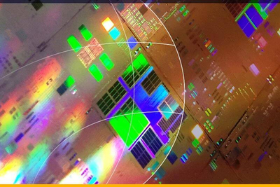
In the semiconductor industry in particular, high-purity crystals have long played an essential role. As the basis for discrete semiconductor components such as transistors and diodes, for microelectronics such as semiconductor memories and integrated circuits and for microsystem components such as sensors and converters, they have to fulfill the very highest standards when it comes to purity and their lattice structure.
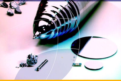
Thanks to its high degree of purity, polycrystalline silicon helps to boost the performance of semiconductors and solar cells. In the polysilicon industry, the Cz process converts polycrystalline silicon into monocrystalline silicon (for semiconductor applications), which is then cut into monocrystalline wafers. These wafers are used as a substrate for electrical systems such as integrated circuits. For solar cell applications, polycrystalline silicon is used as a base material for producing crystalline silicon solar cells.